


 返回
返回 下载
下载MARIE FREEBODY, CONTRIBUTING EDITOR
Micro-optics are a key enabler in the modern world, spurring advancements in consumer electronics, automotive lighting, and the next generation of autonomous vehicles. As demand grows from sectors far and wide, new fabrication approaches — some borrowed from the microchip industry — are allowing for faster and more economical production.

A car with microlens array (MLA)-based headlights. Such headlights provide the freedom to create a distinctive vehicle exterior with a slim appearance while at the same time reducing weight, packaging size, and power consumption. Courtesy of SUSS MicroOptics.
One catalyst for the expansion of the micro-optics market has been the advent of new light sources over the last 25-plus years. These include excimer lasers for photolithography, high-power laser bars for industrial manufacturing, laser diodes for fiber optic communications, and VCSELs and LEDs.
Micro-LED and mini-LED arrays, extreme superluminescent diode laser lights, and other new light sources are all expected to spur the development of additional applications and open new markets for micro-optics, which collimate, shape, and couple light.
Automotive lighting is one example of a new market for micro-optics. The first two serial-production cars using microlens array (MLA) headlights are on the road, but it is an open question when other automakers will follow suit, given the conservative and cost-driven nature of the auto industry.
“MLA headlights achieve top ranking in saving space, energy, and material, and allow full design freedom for car designers,” said SUSS MicroOptics CEO Reinhard Voelkel. “Lighting is considered to be the ‘new chrome,’ yet it’s not so easy for a novel technology to be accepted as a new industry standard.”
Other consumer markets for micro-optics include microdisplays for augmented and virtual reality (AR/VR) headsets and head-up displays, as well as positioning and communications systems for autonomous vehicles, architectural lighting and displays, and smart electronics.
Consumers are also demanding evermore powerful smartphone cameras — a market that, by itself, is driving the manufacture of several billion camera assemblies every year. As these cameras become increasingly sophisticated, their assembly tolerances grow smaller.
With such lucrative markets, the clamor for components that do more in less space has micro-optics-makers investing heavily in scalable manufacturing options, high-refractive-index polymers, and speedy alignment.
Cost-effective volume production
As investment pays off and fabrication improves, this in turn drives down the cost of production and enables wider adoption in the marketplace. The positive feedback loop is hampered only by a sometimes lengthy initial prototyping stage, during which achieving repeatability at a marketable price point is the biggest challenge.
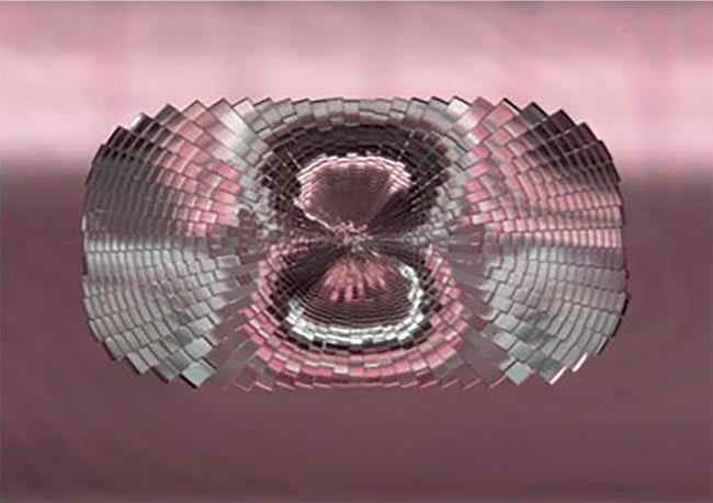
Although a variety of fabrication techniques are in use today, the most advanced is wafer-level manufacturing. In this method, microlens arrays are constructed by either photolithography and plasma etching; imprint or replication involving polymer on glass; or grinding, polishing, wet-etching, or a similar process on full wafers.

A car with external light projections (bottom). MLA-based projections can be mounted into the smallest of spaces under a car, enabling unique external designs coupled with lightweight, powerful, and shaped illumination that is ideal for safety features and light carpets. MLAs for external automotive light carpets. Courtesy of SUSS MicroOptics.
One class of micro-optics — wafer-level optics — is manufactured in much the same way as microchips. But, instead of thousands of microchips on a wafer, thousands of lenses are manufactured on an industry-standard 8-in. substrate. Simultaneous processing of several thousand optics on a large wafer is essential to meet the demand of dynamic, growing markets. But unlike semiconductor production, micro-optics fabrication remains at a much lower degree of industrialization and automation and is encumbered by a large number of manual processing steps.
These limitations may, in part, be due to a relatively small number of players in the micro-optics sphere, as well as the diversity of fabrication methods. Fully automatic, off-the-shelf production equipment is available for only a few of the steps.
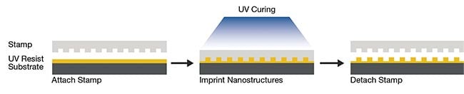
A UV nanoimprint lithography process flow. A substrate is spin-coated or drop-dispensed with a UV-curable resist. Subsequently, a stamp is pressed into the resist and cross-linked by UV light while still in contact with the resist. Courtesy of EV Group.
For wafer-level production, a critical challenge is to maintain or even improve the performance and quality of optical components over a large area while reducing the cost per area by decreasing the time spent on each part. Performance testing at the wafer level achieves these goals by reducing handling time and simplifying process monitoring — as it did for microelectronics production.
“The scalability of the processed substrate size-per-time, sequential, or batch processes, or continuous processing in roll-to-plate or roll-to-roll are already adopted to deliver large quantities at lowest cost,” said Dirk Hauschild, head of R&D at Focuslight Technologies Inc.’s laser optics business unit.
“The next major game changer will be production of a product with a defined performance with a simpler material on a larger substrate, similar to what the flat panel display industry has done in the past 20 years,” he said.
Nanoimprint lithography
Nanoimprint lithography (NIL) lends itself well to high-volume production by using UV light to transfer lens patterns onto optical polymer materials in tandem with working stamps that are replicated from wafer-size master stamps.
EV Group of St. Florian, Austria, has amassed over 20 years of experience in nanoimprint technology. The company invests heavily in high-precision alignment techniques to increase the number of microlenses that can be manufactured on a single wafer.
“NIL offers flexibility in terms of shapes, dimensions, sizes, and overall design freedom,” said Andrea Kneidinger, EV Group’s business development manager. “The technology can replicate sophisticated structures very efficiently, on large areas, with few design constraints, and with a very streamlined process flow, for both prototyping and high-volume manufacturing.”
Unlike other lithography techniques that are reaching their resolution and/or cost limit, NIL enables high-resolution capabilities for complex lens designs, without added manufacturing costs. The method is also compatible with a broad range of materials, including standard optical, high- and low-refractive-index, biocompatible, and etching materials.
“In recent years, many improvements were made to the NIL process for micro-optics fabrication,” Kneidinger said. “For example, alignment accuracy has continually improved, to the point where EV Group can reach 300-nm alignment, a new industry benchmark.”
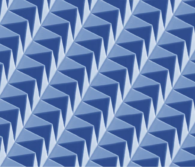
Fifty-micron-wide structures are replicated using EV Group’s nanoimprint lithography solutions. Courtesy of EV Group.
Another important advancement has been wafer-level processing, she said, where NIL can create 2.5D or 3D structures — such as diffractive optics, nanogratings, diffusers, beamsplitters, and even metalenses — in tight formation on a glass wafer all at one time, enabling the processing of hundreds or thousands of microlenses in parallel.
Subsequent processing steps such as coating, precision stacking, and etching can also be carried out at the wafer-level, meaning the complete optical module is manufactured efficiently, Kneidinger said.
This higher level of efficiency has led to new consumer devices for 3D sensing, biometric authentication, and spectral imaging that are being integrated into high-volume products such as smartphones.
Miniaturization as multiplier
Demand for smaller, faster, lighter, and cheaper products continues to put pressure on the entire supply chain. The companies that can figure out how to do either more in the same space or more in less space will realize the most significant gains in the marketplace.
For component suppliers, microinjection molding has proved a key technology for innovation. Microinjection molding focuses on microsize parts (typically 1 cm and smaller) with microsize features (some measured in microns), and microsize tolerances (in some cases ±2 µm).
“It sounds cliché, but miniaturization is still one of the most significant trends in the industry today,” said Aaron Johnson, vice president of marketing and customer strategy at Accumold. Miniaturization provides more functionality, more discrete capabilities, and efficient designs, he said. But as the miniaturization trend continues to push the parameters of size and quality, the demand is on the rest of the supply chain to keep up. This includes not only suppliers of high-precision injection molding for polymer optics, but also other supply chain partners, such as resin suppliers.
“Many are looking for polymers that not only can be made into micro form factors but can also withstand high-heat applications like three-times solder reflow processes,” Johnson said. “This puts a lot of pressure on the full supply chain to figure out the right combinations for these demands.”
Picking the right supply chain partner is crucial when a company is pushing the limits of its own technology.
“It’s beyond just capability,” he said. “It’s finding a partner that can scale with you and be with you for the long haul. Some projects may only last 18 months; some last years. Partner with suppliers that can truly partner with you no matter the need.”
Freeform micro-optics open new markets
The large-scale manufacturing of freeform micro-optics — which embraces the remarkable capabilities of freeform optics but in a smaller form factor — has exhibited huge growth. This is of particular interest for the AR market, where glasses need practical form factors to see broader adoption by consumers.
Growth is evidenced by an exponential surge in patents for and papers on freeform micro-optics. This growth is expected to continue for at least the next 18 months to three years, according to Jessica van Hck, managing director of the PHABULOuS Pilot Line.
“The biggest advantage is the increased freedom of design,” van Heck said. “Combining the advantages of freeform optics with a small form factor is opening up many possibilities for miniaturization and improved aesthetics. But it also enables energy-saving solutions, for example, by using foils with microstructures on luminaires to create the same or better light distribution using fewer LEDs.”
An example of micropolymer optics. These parts, molded out of Ultem (polyetherimide), are part of a complex datacom connector. The geometry includes 12 Ø 250-µm lenses with a ±2-µm positional tolerance. The parts also include V-groove alignment features and a turning mirror that must also meet the exacting standards of the design. Courtesy of Accumold.
The executive team at WaveFront Technology Inc. agrees. For CEO and CTO Chris Rich, president and CFO Joel Petersen, and COO Kent Coulter, the advancements in freeform optics, materials, and computational power mean that micro-optics is pushing beyond current lighting standards.
“In other words, we cannot anticipate what is next by what we currently experience naturally. It can now be better,” Rich said.
Examples of recent advancements include LED lighting fixtures that incorporate micro-optics to create patterns that give the appearance of depth and movement, or illuminate and accentuate a particular area. To achieve these effects, freeform optics are coupled with advanced polymers that have been chemically engineered to exhibit a wide-ranging index of refraction.
“To expand the range from low to high index of refraction, the incorporation and stabilization of additives such as fluorine, sulfur, and metallic nanoparticles in organic systems has been the primary method,” Petersen said. “In many cases, these are extensions of existing polymer families. These have been desired materials in the optics communities for many years, and the advances in the abilities to use them, and the market adoption of products that take advantage, appear to be coalescing to make investment in development attractive.”

Focuslight’s blue diode laser optics are used for high-absorption materials processing, medical treatments, lighting via phosphors, and as a pumping source for specific crystals, and more. Courtesy of Focuslight.
Unlike standard optics, freeforms pose particular manufacturing challenges — not just in what becomes possible to make, but also in scalability. The involvement of multiple companies is often required for the design, origination, and replication of freeform optics, and possibly also for integration and coatings.
“When looking at freeform micro- optics, the design for manufacturing plays a huge role. Understanding the capabilities and limitations along the value chain is very important,” van Heck said. “We have created a platform for different suppliers in the value chain to work together and have developed software to quickly identity how to improve the manufacturability of a design.”
Addressing packaging challenges
Scale-up and incremental improvements in fabrication are expected to continue at a steady pace. An important challenge arises in the next step — packaging, in which alignment of micro-optics into ever smaller modules or systems is arguably the single biggest cost driver in the production of photonic devices.
Reducing this dominant cost will fuel end-market applications because such a reduction will facilitate profitability and affordability, as well as enable rapid scaling and flexible manufacturing.
For at least the last three decades, there has been a push to develop passive alignment techniques for photonic and micro-optical assemblies. In passive alignment, each element is fabricated to the necessary nanoscale precision so that the elements can be snapped together like Legos.
SUSS MicoOptics’ Voelkel believes that the micro-optics industry could actively reduce packaging challenges for its customers, for both passive and active alignment, by adding additional features such as alignment marks, prisms, vias, V-grooves, and monolithic integration of microlenses and prisms.
“The wafer-level process can handle this increased complexity very efficiently and thus reduces the complexity for the customer during system integration,” he said.
Scott Jordan of PI (Physik Instrumente) agrees that passive alignment has its place, but he believes that active alignment will increase in importance and that, by reducing the cost and time taken, the need for passive alignment will be reduced.
“Because alignment itself is so time-consuming, and because alignment must be repeated at multiple steps, a hundred-fold reduction in that cost, times multiple steps, is very, very significant,” Jordan said.
For the increasing number of micro-optic assemblies requiring submicron tolerances, manual alignment proves too time-consuming to be able to scale up to the quantities being forecast in the next few years.
The microchip sector reveals an obvious solution: automation.
“When you are confronted with a wafer containing thousands of elements that need to be assembled — whether lenses or chips — it really adds up,” Jordan said. “This is what PI targeted and addressed with our intelligent microrobots and stage assemblies that can automatically detect and optimize alignment of micro-optic or photonic parts.”
The company uses a hexapod design to provide multiaxis motion in conjunction with firmware-based algorithms to perform high-speed alignment of lenses, silicon photonics, or arrays. The result is a flexible active alignment system that is typically 100× faster than its previous technologies.
Prototypes fit for commercialization
One prototyping planning error in particular is probably the biggest barrier to commercialization: Many good ideas fail to make it to market because their developers miss the opportunity to prove that a single prototype could be scaled to the necessary volumes.
Often, single lenses, microlens arrays, diffractive optics, nanogratings, diffusers, beamsplitters, and homogenizers are designed or even made available at the die level but are too costly to produce on larger scales.
A master with a freeform microstructure used to redistribute light from LEDs, which improves light distribution in a smaller overall system. Courtesy of PHABULOuS.
Close cooperation between the optical solution designer and the production toolmaker is critical to maximize the range of optical functions of a product that can be manufactured at scale. Many firms actively facilitate close partnerships to overcome this challenge.
Examples of cooperation models in operation include EV Group’s NILPhotonics Competence Center and Focuslight’s Center for Optical Research and Engineering (CORE). At CORE, micro-optical solutions come from combining the requirements for optical design, production technology, and application performance. These three pillars also guide the development of products.
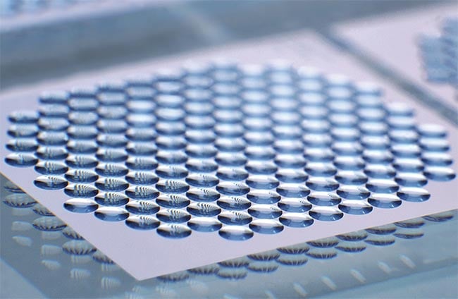
Wafer-based production technology produces polished wafers up to 300 × 300 mm, making it possible to produce tens of thousands of lenses from high-grade glass and crystal in a single process step with a consistently high level of quality. The surface shape of each lens can be individually designed to yield the best intensity distribution, while precision manufacturing on a wafer basis provides a high rate of repeatability and reproducibility. Courtesy of Focuslight.
“The limited level of standardization in micro-optics and photonics always needs application and customer-specific designs and configuration that need some extra efforts during the design and production phases to make use of all advantages of the design, especially for initial small and medium quantities,” Focuslight’s Hauschild said. “Balancing the performance, integrability, and cost structure linked to the applications can often only be solved by the adaptation and modification of fabrication techniques that achieve a better total solution than using existing standard production tools.”
As close collaboration helps to deliver prototypes to market, the parallels to the semiconductor industry look to continue. Faster and cheaper prototyping is likely to benefit from advancements in 3D printing. Just as microchip-makers are increasingly embracing the technology, 3D printing will also aid micro-optics design engineers.
“Prototyping through high-accuracy 3D printing by two-photon polymerization and mastering capabilities, like ultraprecision machining, will lead to much faster time to market and lower entry barriers in the future,” SUSS MicoOptics’ Voelkel said.