Presentations and Poster
1. A novel electrochemical corrosion resistant solution for water-cooled diode laser stack
Date: 18 January 2026 • 16:30 - 16:50 PST
Location: Room 208 (Moscone South, Level 2)

Speaker: Dong Hou is Manager of Process Engineering and Material Team at Focuslight. He has over 12 years of experience in high-power diode laser device development and packaging, holds more than 30 patents, and has published over 15 technical papers in SPIE and other photonics journals.
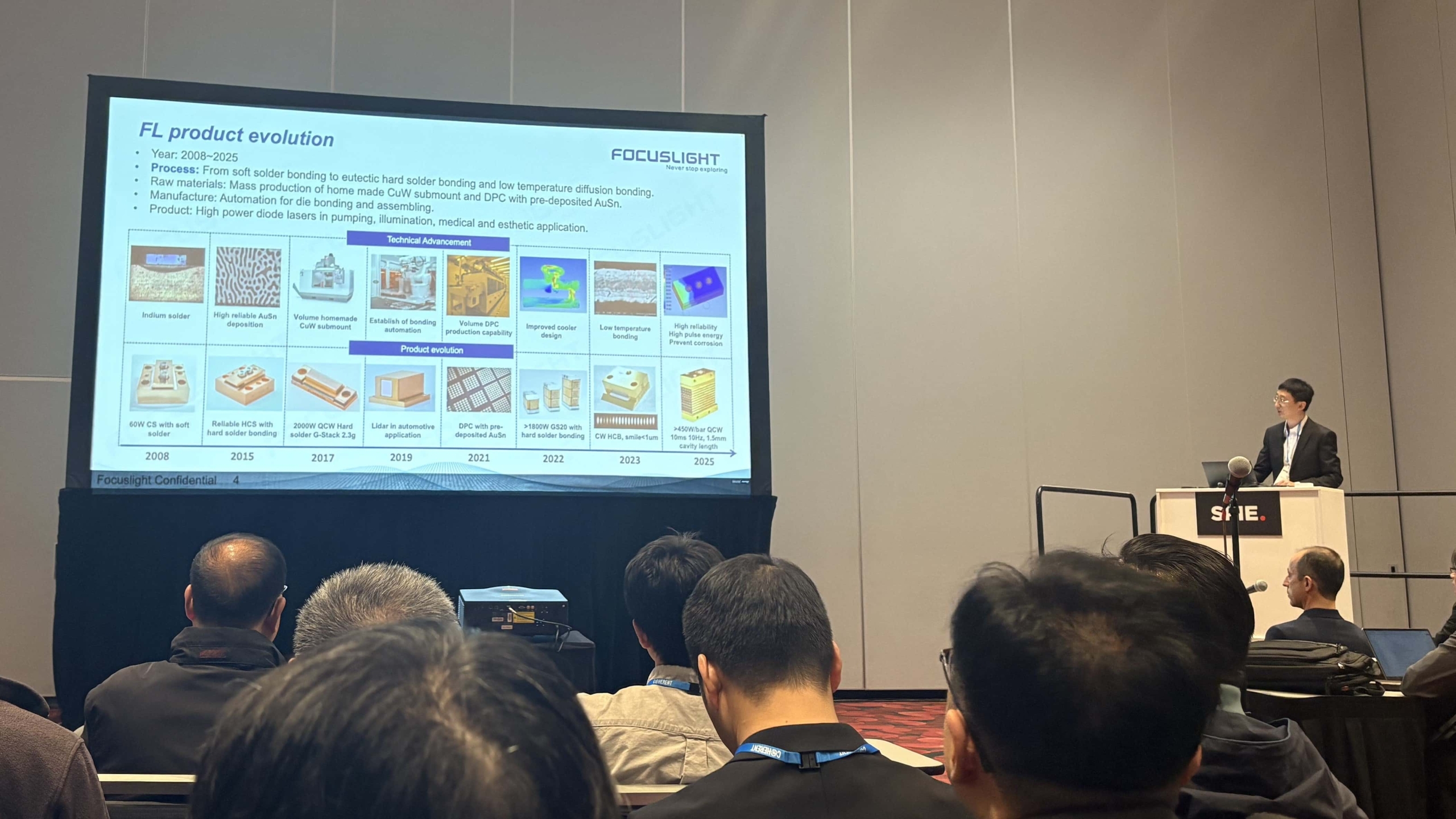
Abstract: Water-cooled high power diode lasers have been widely applied in the field of medical health, industrial processing, and scientific research. Normally diode laser bars are bonded onto copper-based water-cooling plates to enhance output power and ensure effective heat dissipation. However, this approach results in electronic drift in water, triggering electrochemical corrosion in cooling plates. This issue manifests as corrosion in the anode channels and deposition in the cathode channels of a stack, ultimately leading to failure due to blockage, leakage, or burning of diode lasers. Research indicates that electrochemical corrosion is strongly correlated with the pH value and ion concentration in the water. Traditional solutions involve complex water treatment modules to maintain stable pH value and low ion concentrations with high cost and large volume. Another approach employs the application of ion exchange resins, which, however, require frequent replacement. In this study, we have proposed combined solutions to reduce electrochemical corrosion, including the protective layers design, reduction of erosion corrosion and improvement of cooler channels. A novel corrosion-inhibiting coolant was applied as an alternative to conventional deionized water without using any water treatment modules. Under these improvements, a 10-bar water-cooled diode laser stack produced by improved large channel cooling plate (LCC) was developed, which passed 3039 hours of quasi-continuous wave (QCW) life-time test without obvious power degradation. In contrast, traditional diode laser stacks using pure water exhibited significant electrochemical corrosion phenomena after 770 hours operation.
2. AI-accelerated high-fidelity volume fabrication of reflow-compatible micro-optics via UV imprinting
Date: 19 January 2026 • 16:45 - 17:05 PST
Location: Room 304 (Moscone South, Level 3)

Speaker: Dr. Libo Yu is Principal Engineer at Focuslight with 12 years of industrial experience in micro- and nano-optical component R&D. He holds a Ph.D. in photonics from EPFL, specializing in micro-optics, and has authored multiple peer-reviewed journal and conference publications.
Abstract: Wafer-level optics (WLO) fabricated via UV imprinting enable scalable, cost-effective production of reflow-compatible micro-optics for compact optical modules in consumer electronics. However, form error (FE) introduced during the manufacturing process—primarily due to polymer shrinkage and mold deformation—necessitates 2 to 3 human-guided compensation cycles, significantly increasing development time and cost. This work presents an AI (artificial intelligence)- accelerated, physics-assisted prediction framework that reduces the development cycles by 30% while maintaining high replication fidelity. We propose a two-step cascaded prediction approach that explicitly decomposes the median FE into a dominant best-fit sphere (BFS) component and a higher-order rotationally symmetric irregularity (RSI), consistent with optical surface standards and physical deformation mechanisms in UV imprinting. In the first step, an AI model predicts the global spherical error as a low-dimensional scalar quantity from single-point diamond turning (SPDT) design parameters. In the second step, this physics-informed prediction is incorporated as an additional feature to regress the full FE profile, enabling focused learning of residual local deformations. The framework is evaluated on 69 distinct micro-optic designs using five-fold cross-validation and benchmarked against conventional single-stage AI models and human-guided compensation cycles. Results demonstrate that the proposed two-step approach achieves up to 3.3× improvement in peak-to-valley accuracy over single-stage prediction and closely approaches the accuracy of second-cycle human correction. Feature-importance analysis further confirms that the cascaded structure successfully decouples global shrinkage-driven deformation from local stress-induced irregularities, providing both improved prediction performance and physical interpretability. These results show that physics-assisted AI can eliminate one full development cycle for challenging designs, offering a practical pathway toward faster, lower-cost, and high-fidelity volume manufacturing of reflow-compatible micro-optics.
3. Next-generation microimprinting: enabling ultraflat base layers for high-end micro-optics applications
Date: 19 January 2026 • 17:05 - 17:25 PST
Location: Room 304 (Moscone South, Level 3)

Speaker: Mirco Altana is Senior Development Engineer and Technical Team Lead at Focuslight. He has over 15 years of experience in cleanroom-based micro- and nano-structuring and has led the development of mastering and imprinting technologies from R&D to high-volume production. His current focus is micro-optics for automotive applications and advanced wafer-level replication.
Abstract: The development and experimental validation of a wafer-scale micro-imprinting system designed to produce ultra-flat polymer base layers for high-end micro-optical components on up to 300 mm glass wafers is presented. The machine combines a high-stiffness force path with nanometer-resolved gap control using multiple interferometric sensors and a programmable dispensing unit for controlled material pre-distribution. To quantify the intrinsic base-layer uniformity, imprint tests with flat, unstructured polydimethylsiloxane stamps of two thicknesses on borosilicate wafers and an epoxy-based UV-curable resin were performed, targeting a 30 μm base-layer thickness. The resulting films were characterized by stylus profilometry along orthogonal wafer axes. Stamp topographies were measured at identical coordinates to allow direct subtraction.
The experiments show that the dominant source of base-layer variation originates from stamp thickness non-uniformity rather than machine mechanics or resin distribution. After correction using the measured stamp profile, the residual wafer-scale variation shows a highly consistent shape for all tested conditions. Different dispensing strategies, from central puddle to star-shaped pre-distribution, change the corrected base-layer uniformity by less than 2 μm, indicating that material distribution is a secondary factor compared to the flatness of the machine chucks.
These results demonstrate that the new imprint system provides a mechanically stable and highly reproducible platform for micro-optical replication in the transitional regime between nano- and micro-imprinting, where uniform base layers are essential for high-quality optical performance.
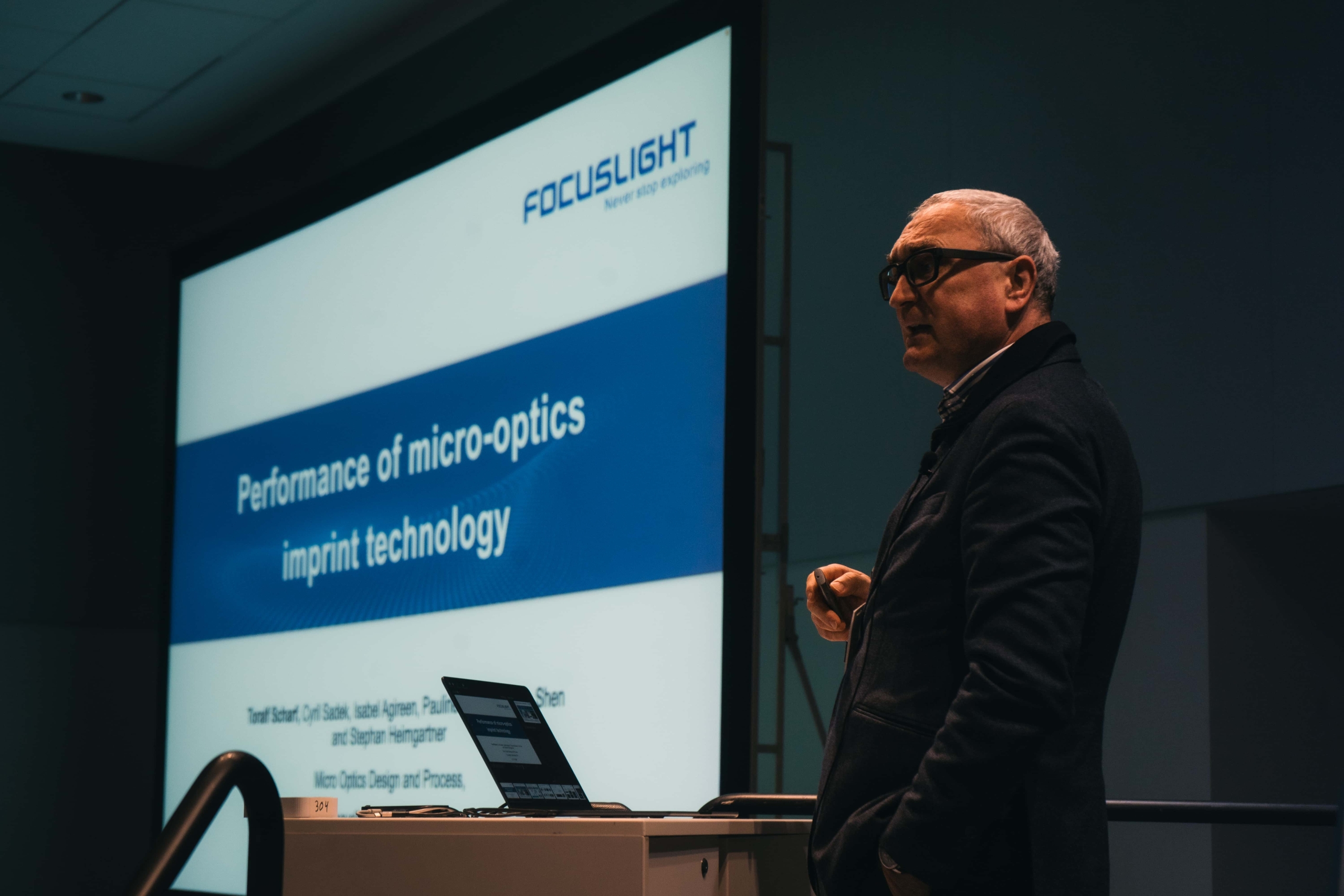
4. Performance of micro-optics imprint technology (Invited Paper)
Date: 21 January 2026 • 10:50 - 11:20 PST
Location: Room 304 (Moscone South, Level 3)

Speaker: Dr. Toralf Scharf is Director of Micro-optics Design and Process at Focuslight. With over 25 years of experience in microtechnology and optics, he has authored more than 200 publications and two books. Before joining industry, he held faculty positions at EPFL and the Institute of Microtechnology in Neuchâtel.
Abstract: Micro-optical components have been getting more and more popular in various applications in projection illumination. Often Microlens arrays are used to realize particular projection functions such as slanted angle street projection. Important is the lens surface definition and the quality of the array with respect to lens position and uniformity. To realize demanding applications of such array projectors the optical surface parameters are most important. Such projectors can contain more than 1000 lenses in a single optical component and if variation of the lens shape gets predominant the optical function will fail. In mass fabrication one has therefore to assure that no deviation happens in the whole fabrication process from mastering to imprint. During the fabrication process of the micro-optical components the surface is subject to geometrical deformations caused by shrinkage and aging of the tooling for instance. Changes are small but relevant and need a complex model that allows to include analysis of optical characteristics. At the quality level of today’s wafer level UV replication process, which can also realize freeform structures a simple analysis of radius of curvature and conic constant is not sufficient. It is therefore important to investigate at which point (or replication cycle) a controlled production is still possible. Only until this point than a correction of the surface shape is still possible. We have implemented an approach using Zernike polynomial fitting which allows us to see all changes down to noise of our metrology toolset and applied the model to a production data.
5. Freeform microlens arrays surface description
Date: 21 January 2026 • 16:50 - 17:10 PST
Location: Room 304 (Moscone South, Level 3)
Speaker: Dr. Toralf Scharf
Abstract: Square and hexagonal footprint shaped lenses made by a wafer scale imprint process, could be a solution the enhance the lens fill factor for applications where imaging is not needed. Additionally, a mastering process using reflow technology will decrease the fabrication costs. But due to their complicated shapes that often need high-order polynomial descriptions for accurate modelling. Models based on the use of Zernike polynomials can help to describe and design the suitable surface for dedicated applications. Some examples will be presented.
6. Stamp material evaluations for next generation wafer level optics (Poster)
Date: 21 January 2026 • 18:00 - 20:00 PST
Location: Poster Hall (Moscone West, Level 2)
Abstract: Polydimethylsiloxane (PDMS) was evaluated, showing some limitations, e.g. swelling due to uptake of low molecular weight species after long time contact with epoxy, and subsequent deformation due to elasticity, as mold material in epoxy imprinting. The authors presented and demonstrated Polypropylene (PP) as potential replacement in wafer level optics (WLO) manufacturing, especially for high end imaging lens, which requires lens form error <0.5um, and position error <5um. With PP mold, the authors have achieved the lifetime of replication >30x, lens form error <0.1um, and roughness <5nm. A new process flow with combining injection molding optics (IMO) and WLO has been proposed.


 Return