Tuesday 4 April 14:00 BST (9 pm China time), Dr. Daniel Braam from Focuslight will be presenting at Electro Optics to talk about Silicon Lenses with Large Sag for Anamorphic Beam-Shaping.
Abstract
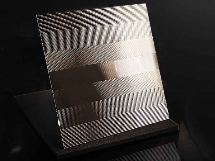
The typical processing technologies of silicon lenses are etching or CNC machining, resulting in the typical lens sag value of <60 µm and not suitable for massive production. Focuslight now expanded its unique structuring capabilities to the mm-scale in silicon, enabling record-breaking silicon lenses. Free-form acylindrical lenses or arrays act on each optical axis separately, creating anamorphic beam-shaping solutions.
With this processing technology, the lens sag can achieve as large as 4 mm (4000 µm) at an exit angle of 0°~80° on silicon lenses, which maximizes the numerical aperture (NA) that silicon lenses could achieve and exceeds the limit of the silicon lenses processed with conventional technologies. This enables products that have been hard or impossible to be produced by classical etching technologies, such as deep-sag decentered lenses, blazed gratings, chirped arrays or integrated prisms, enabling innovative, highly cost-effective, and scalable core component solutions for next-generation silicon photonics, enabling biosensing, PICs, and much more.

Silicon Lenses with Large Sag
Key features:
- Silicon: High IR transmission
- High refractive index (n=3.4)
- Free-form shape in one direction: asymmetric, decentered lenses, arrays & prisms
- Large sag, wide exit angles
- Polished surfaces
- In-house coating with R<0.2%
Applications:
- Detection and beam-shaping of IR light/energy
- High transmission efficiency for compact sensor applications
- Telecom & direct photonic integration
Speaker

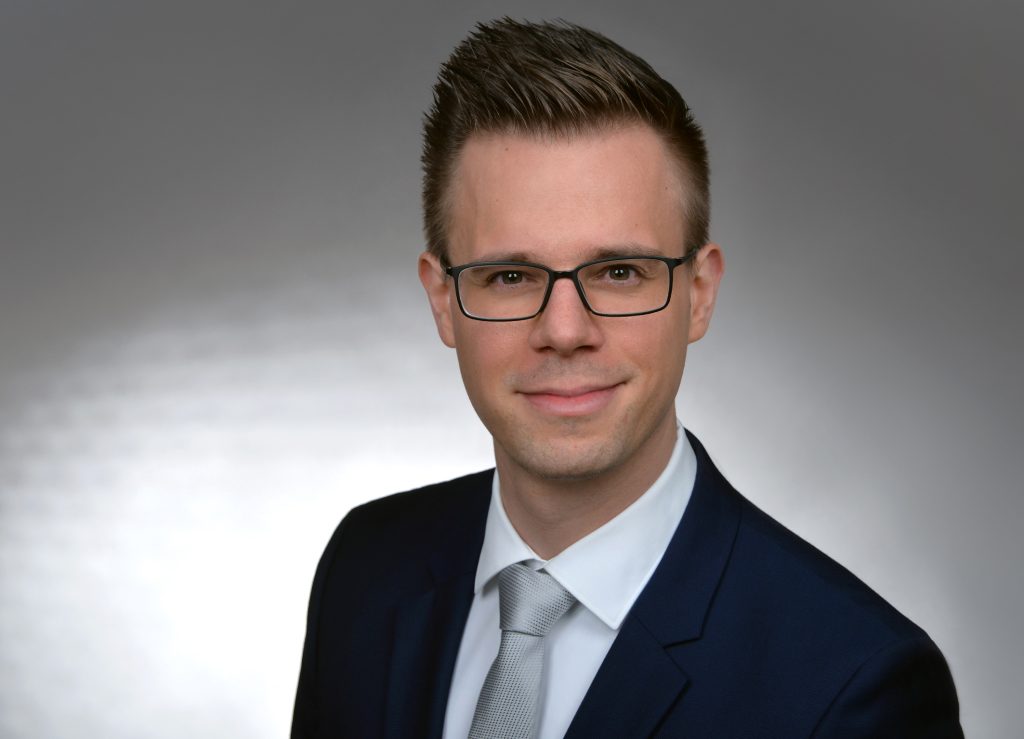
Dr. Daniel Braam has been Head of Product Line Management for micro-optics at Focuslight Laser Optics Business Unit since 2018. He studied physics and received his PhD at the University of Duisburg-Essen in the field of optics and nano-structures. He has contributed to over a dozen publications for high-impact journals.
About Focuslight’s Wafer-level Simultaneous Structuring Technology
At Focuslight, optical components are manufactured on a wafer base with Focuslight’s own wafer-level simultaneous structuring technology, which is applicable to any kind of inorganic optical material. From CaF2 and MgF2 crystals, to high-grade fused silica or high-index glasses, to semiconductor-industry quality Si and Ge material, the wafer-based products cover a wide range of wavelengths from DUV to FIR, structuring optics with nearly unlimited complexity of 1D acylindrical and prismatic surface geometries. Especially (but not exclusively) for silicon, this includes optical and mechanical features for alignment and assembly, opening up the opportunity to implement the products for optomechanical and optoelectronical functionalities.


 Return
 Download


