Originally published in Photonics Spectra, (Oct 2020)
炬光科技Activation系列高功率半导体红外线光斑激光系统多年来广泛应用于工业领域,本文介绍了激光非接触式加热在显示行业的应用,由炬光科技产品经理顾维一等撰写,原文发表于《Photonics Spectra》十月刊。
文章概要如下:
异方性导电薄膜(ACF)在显示行业组件封装中的应用已有20多年的历史,通过使用ACF键合,零件通过含有导电颗粒的胶膜进行电气和机械连接。在键合过程中,通过控制热量、压力以及作业时间,辅以零件位置控制,可达到机电连接牢固可靠的目的。
但随着显示技术的不断发展,在更紧凑的区域(如柔性显示屏的极窄边框内部)完成ACF键合工艺成了新的技术方向。在实际工艺中,由于传统接触式加热的热压头体积较大,无法完全满足极小区域的键合需求。炬光科技Activation系列产品通过设计适配的光斑尺寸、能量密度和工艺曲线,完成对键合区域的快速加热,从而达成键合工艺,在ACF键合应用中拥有很大潜力。
Emerging display designs favor more screen and less frame, prompting interest in noncontact thermal bonding tools powered by diode lasers.
WEIYI GU, KEVIN ZHU, AND JOANNA QIAO,
FOCUSLIGHT TECHNOLOGIES INC.
The display industry has used anisotropic conductive film (ACF) for component packaging applications for decades. By aligning display parts precisely and applying heat and compression for the right duration of time, ACF bonding technology ensures strong and reliable electrical-mechanical interconnections. Further, the characteristics of ACF make it possible to form electrical and mechanical bonding in a single step.
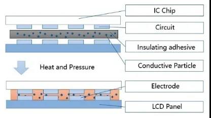
A typical anisotropic conductive film (ACF) bonding process for LCD panels. IC: integrated circuit. Courtesy of Focuslight.

With the addition of beam shaping and homogenization by micro-optics, diode lasers offer highly controllable spot size, extremely high-energy uniformity, and high energy density, which all contribute unique benefits in display manufacturing. Courtesy of Focuslight.
New developments in display technologies are requiring ACF bonding processes to be applied within a much smaller area, such as the extremely narrow frame of a flexible display. The bulky size of conventional thermal heads makes these bonding applications infeasible, which has prompted a growing interest in noncontact laser heating tools. Such tools offer flexible beam size, energy density, and process curves to enable an alternative rapid, noncontact bonding process.
ACF bonding
ACF bonding is a packaging technology that is widely used in manufacturing processes for LCDs, organic LEDs, and active-matrix organic LED panels.
The films comprise a mixture of resin and conductive fillers such as nickel particles or nickel-gold-coated polymer beads to enable z-direction conduction and insulation between terminals. In display manufacturing processes where high-temperature soldering might adversely affect product reliability, ACF offers a relatively low-temperature (≤180 °C) bonding alternative. ACF bonding is widely used to bond flexible printed circuits or chips to LCD panels, for example.
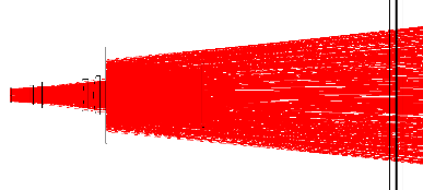
An example of light distribution in an ACF bonding process as provided by an optical design for a 300- × 3-mm laser beam. Courtesy of Focuslight.
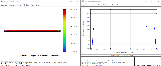
Beam spot and energy distribution of the 300- × 3-mm laser beam. Courtesy of Focuslight.
ACF can connect two materials with different characteristics and form a stable electrical connection along the z direction while maintaining electrical insulation in the xy directions. The blend of thermoplastic elastomer and thermosetting epoxy polymer can provide electrical insulation, protect metallic contacts from mechanical damage, ensure stable adhesion between two materials, and provide good moisture and corrosion resistance.
In mature applications, material curing with contact pressure applied by heat press plates is a stable and reliable solution. Packaging technologies such as film on glass, chip on flex, and chip on glass have been widely used.
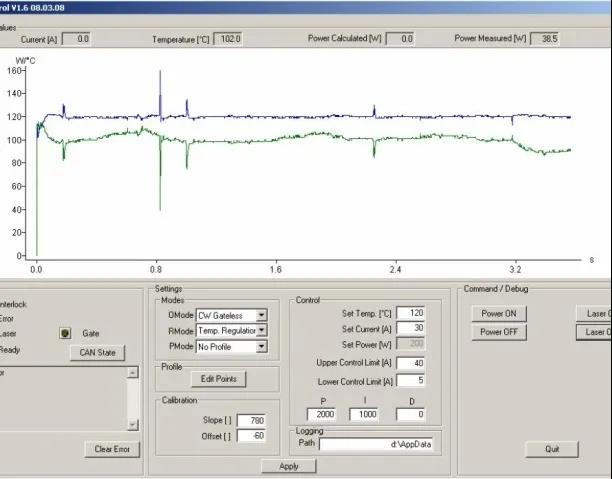
Combined with closed-loop controls, the output power of diode lasers can be adjusted in real time to ensure good temperature stability during the entire bonding process. Courtesy of Focuslight.
However, ongoing developments in the display industry continue to increase the screen-to-body ratio of displays for personal computers, mobile phones, tablets, and smart devices. Meanwhile, the frame size of displays continues to decrease, as well as the bonding pitch between the LCD and tape carrier package (TCP).
Traditional material curing methods using contact pressure can no longer meet the processing needs for these display designs for several reasons. First, the size constraints of the heat press plates used, their uneven heat distribution, and the thermal expansion of the material can all lead to backlight bleed issues in LCD panels processed with contact pressure cure methods. Second, the temperature rise time of heat press plates is relatively long, extending bonding process time, and the excessive heat accumulation also reduces manufacturing yields. Third, as display dimensions expand, demand for simultaneous bonding at multiple positions has emerged, and it is difficult to ensure consistent bonding at each position with the traditional curing processes.
Laser-based bonding
Lasers have been widely used in the industrial sector for decades and continue to upgrade and replace traditional processing technologies. Suitable for materials processing applications such as cutting, bonding, drilling, marking, and annealing, lasers have become more and more important for high-tech manufacturing.
As the laser type with the highest wall-plug efficiency, diode lasers offer special characteristics. Specifically, edge-emitting high-power diode lasers offer large divergence angle and uniform energy density distribution. With the addition of beam shaping and homogenization by micro-optics, they also produce a laser spot with controllable size, extremely high-energy uniformity (>95%), and high energy density (kW/mm2). These characteristics all contribute to a solution that is able to meet the needs of different display manufacturing applications.
The controllable spot size and other features of diode lasers also offer a unique noncontact heat source that has introduced an alternative to conventional ACF bonding process. Implementation of this new process requires several considerations to laser design and process control.
Bonding materials and laser wavelength. The thermosetting resin used in ACFs plays an important role in the bonding process and determines the bonding strength between the TCP and indium tin oxide (ITO) glass. The resin hardens when the temperature of the ACF increases to the curing temperature, and thus generates strong peel strength. In real-world applications, common ACF materials have good absorption for wavelengths between 800 and 1000 nm. Infrared diode lasers emitting in this range can heat the material to curing temperatures (170 to 200 °C) in a short time.
Design of the laser spot. Manufacture of large displays usually requires multiple soldering positions on each side of the panel — typically 4 to 6 chips on the long side of a 14-in. LCD display, for example. Achieving simultaneous bonding at each position requires application of a laser line beam with masks as the heat source. Adjusting laser power and energy density helps ensure uniform energy distribution across multiple positions for consistent and reliable bonding.
Uniform line beam. One effective approach to achieving line beam uniformity employs an infrared diode laser vertical stack with output power of up to 4 kW as the heat source. The stack is soldered with low smile, a form of bonding that can significantly improve the ability to achieve beam uniformities greater than 95%. The emitted light is collimated first with fast-axis and slow-axis lenses, and again with additional collimators to reach a desired spot size. A reflective optical element designed for high power density further homogenizes the light beam. This configuration produces a laser line beam uniformly measuring 300 mm long and 3 mm wide and focused at the correct working distance for ACF heating applications. The rectangular beams produced exhibit more than 98% uniformity in both directions. Various masks can be applied to the line beam to meet bonding requirements of areas with different sizes.
In-process temperature control. Monitoring and controlling temperature is necessary to ensure reliable bonding using heat press plates. Typically, temperature sensors on the contact thermal head perform this role. When using diode lasers, however, heat can accumulate fast, and the temperature change of the material can be relatively rapid. Infrared temperature sensors with a sampling rate of 1 kHz or higher are often used for long-distance temperature measurement in such applications. Combined with closed-loop controls, the output power of the laser can be adjusted in real time to ensure good temperature stability during the entire bonding process.
Design of the laser bonding process. The heat generated by diode lasers is concentrated, allowing most of the energy to pass through the ITO glass and interact with the ACF material directly. Compared to traditional heat pressing processes, a thermal head with a constant temperature is retained on top of the TCP while the thermal head under the ITO glass is replaced with a high-strength and high-permeability quartz material.
During the laser bonding process described, the ACF material is first attached to the electrode surface of the glass substrate or TCP, and then the TCP electrode is pre-aligned with the glass substrate. The upper thermal head is headed to 80 °C before applying 0.5 MPa/cm of pressure to the material. A high-accuracy camera ensures the head is precisely aligned.
At this point, the laser is activated to quickly heat the ACF material layer from the bottom to achieve curing temperatures between 180 and 200 °C in a short time. During this period, the curing pressure is increased to 3 MPa/cm and maintained until the curing process is complete.
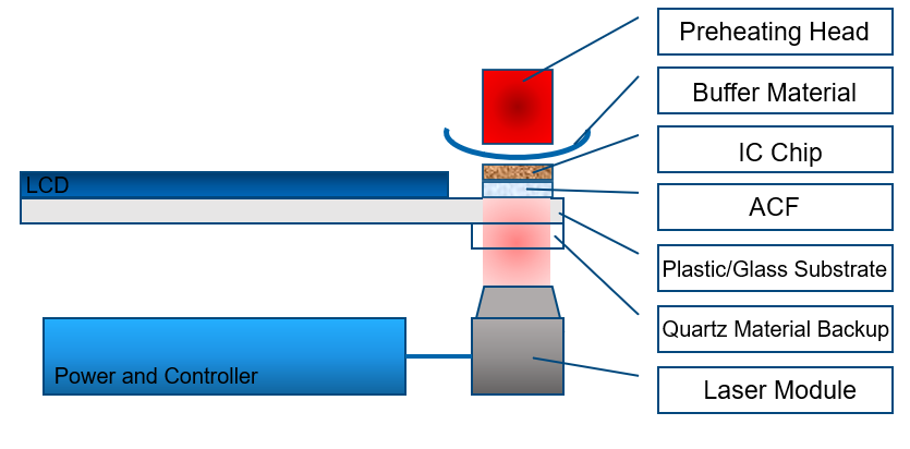
A laser-based ACF bonding system design. Courtesy of Focuslight.
Laser-based anisotropic conductive film material curing processes can reduce the processing time of traditional contact heat press methods due to their unique noncontact heating capabilities and high instantaneous heat output. The laser-based ACF bonding process described is particularly suitable for large-size displays with a small bonding pitch and a long bonding length, making it an attractive solution as the display industry continues to evolve.
Meet the authors
Weiyi Gu is senior manager of laser systems at Focuslight Technologies Inc. He focuses on the process and product development of high-power diode lasers for industrial applications. Gu has a master’s degree in engineering from Xi’an Technological University; email: guwy@focuslight.com.
Kevin Zhu is sales director of laser systems and optical systems at Focuslight Technologies Inc. He previously worked for Coherent/ ROFIN, Continental, and Philips. Zhu has a master’s degree from Toulouse Business School in France; email: zhuyk@focuslight.com.
Joanna Qiao is senior marketing manager at Focuslight Technologies Inc. She began her career at the company as a sales engineer. Qiao has a master’s degree from Humboldt University of Berlin; email: qiaoj@focuslight.com.
关于炬光科技:
西安炬光科技股份有限公司成立于2007年,是一家全球领先的专业从事高功率半导体激光器、激光微光学元器件、光子技术应用解决方案的研发、生产及销售的国家级高新技术企业。公司围绕光子技术及应用领域,致力于为全球客户提供高功率半导体激光器与激光微光学核心元器件及光子技术应用解决方案,形成了全面、完善的研发、生产及销售服务体系。


 Return
 A typical anisotropic conductive film (ACF) bonding process for LCD panels. IC: integrated circuit. Courtesy of Focuslight.
 With the addition of beam shaping and homogenization by micro-optics, diode lasers offer highly controllable spot size, extremely high-energy uniformity, and high energy density, which all contribute unique benefits in display manufacturing. Courtesy of Focuslight.
New developments in display technologies are requiring ACF bonding processes to be applied within a much smaller area, such as the extremely narrow frame of a flexible display. The bulky size of conventional thermal heads makes these bonding applications infeasible, which has prompted a growing interest in noncontact laser heating tools. Such tools offer flexible beam size, energy density, and process curves to enable an alternative rapid, noncontact bonding process.
 An example of light distribution in an ACF bonding process as provided by an optical design for a 300- × 3-mm laser beam. Courtesy of Focuslight.
 Beam spot and energy distribution of the 300- × 3-mm laser beam. Courtesy of Focuslight.
ACF can connect two materials with different characteristics and form a stable electrical connection along the z direction while maintaining electrical insulation in the xy directions. The blend of thermoplastic elastomer and thermosetting epoxy polymer can provide electrical insulation, protect metallic contacts from mechanical damage, ensure stable adhesion between two materials, and provide good moisture and corrosion resistance.
In mature applications, material curing with contact pressure applied by heat press plates is a stable and reliable solution. Packaging technologies such as film on glass, chip on flex, and chip on glass have been widely used.

 A laser-based ACF bonding system design. Courtesy of Focuslight.
Laser-based anisotropic conductive film material curing processes can reduce the processing time of traditional contact heat press methods due to their unique noncontact heating capabilities and high instantaneous heat output. The laser-based ACF bonding process described is particularly suitable for large-size displays with a small bonding pitch and a long bonding length, making it an attractive solution as the display industry continues to evolve.


