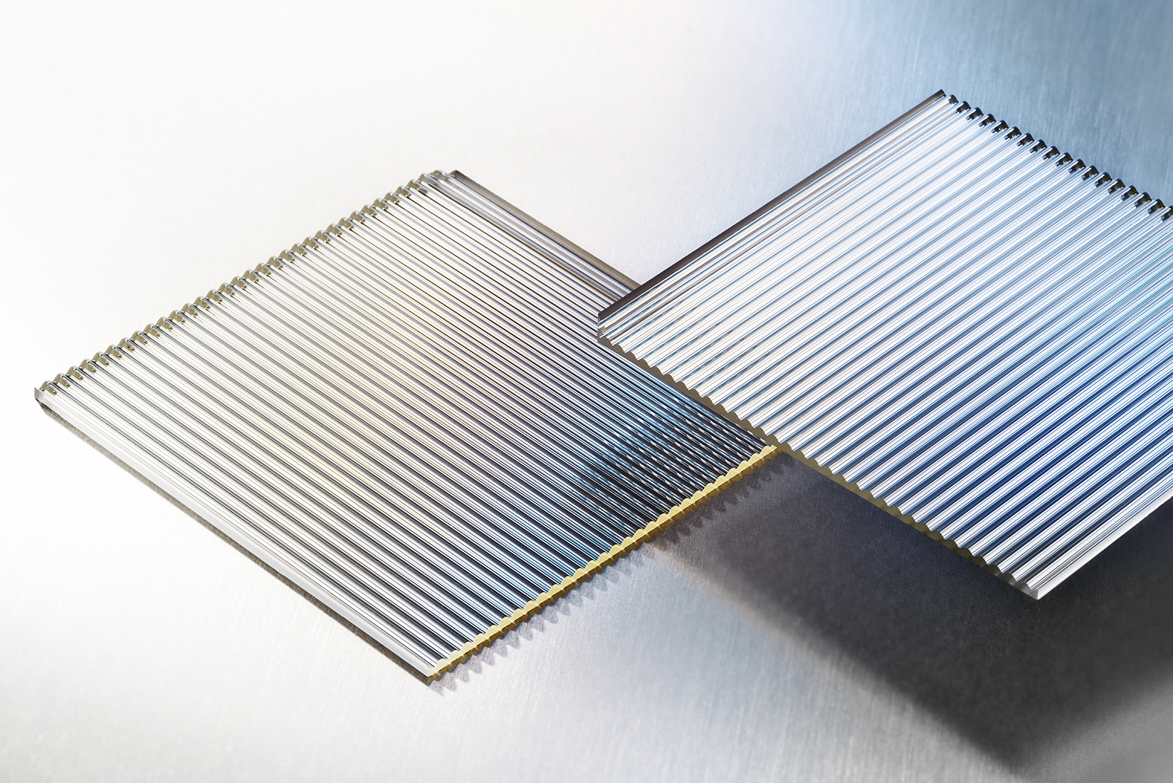
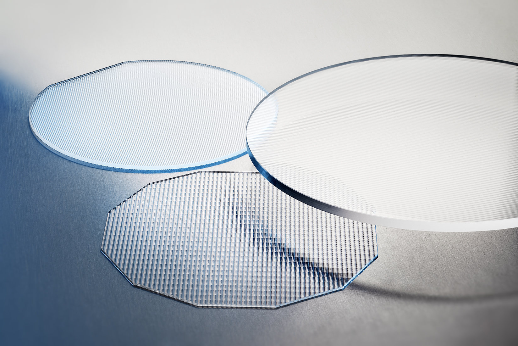
1. The definition of micro-optics
Micro-optics, which was born in the 1990s, refers to a discipline of design, preparation, and application of optical components and systems with micron and nanometer micro-structures.
With the development of microfabrication technology in the semiconductor industry, many new applications with new features are generated just by miniaturization and combining a variety of functions in a small area. This has led to the need for miniaturization of optics to handle new applications in fields of optics, lasers, and beyond.

In addition to imaging, focusing and other pure optical functionality, micro-optics can also achieve refraction, reflection, and diffraction. The possibility to produce micro-optics on wafer level introduced the possibility to produce not only several single lenses at the same time but also to produce lens arrays with 1D and 2D light shaping functionality.
And finally, the combination of optical and mechanical features in one element opens a completely new field of small optics and optical systems that help us today in all fields of application from industry to consumer applications.
2. The applications of micro-optics

The following examples show some prominent break-through in the industry using micro-optics that changed finally the way we live, communicate and work in the 21st century:
Laser material processing using semiconductor pumped laser
In the field of material processing, such as the production of metal parts in all industries including the demanding automotive industry with ultra-stable and lightweight constructed car bodies, high-power fiber and DPSSL laser are increasingly widely used.
The use of the most efficient diode laser sources in combination with FAC, SAC and BTS is an important part of the production of high-power fiber and DPSSL laser.
Microelectronics using optical immersion lithography
The use of immersion lithography with micro-optics enhanced mask illumination is the basis for a still creasing transistor density of semiconductor devices with today 1TB on a few mm² silicon or SoCs with a computer fully integrated into one chip.
Micro-optics provides an optical field homogenizer for a semiconductor photolithography machine. The excimer of photolithography is homogenized on a silicon wafer, making photolithography achieve high precision and high resolution.
Scale application of flexible display with laser stripping technology
Line-beam shaped UV and IR laser improves the performance and functionality of materials used for high-resolution displays and helps to lift of flexible displays for a glass substrate with a contact-free optical separation process that would be impossible with regular mechanical separation processes.
In the OLED manufacturing process, the technology based on micro-optical shaping can form a line spot with a high energy density of 20-30 microns wide, 750mm or even longer by deep ultraviolet laser. Through scanning, the flexible display film layer can be separated from the glass substrate without contact.
LiDAR and AI applications
Light structured and shaped laser with micro-optics enables compact and reliable optical devices that can be used to confirm your ID and to measure precisely the position of your car in the traffic and bring you to your destination safe and relaxed.
According to the difference of LiDAR scheme, laser sources can be collimated and compressed on the fast and slow axes respectively through fast axis collimation and slow axis collimation, thus improving the angular resolution of LiDAR in two directions. The point light source can also be shaped into a very wide line light source, which can form a large field of view angle through scanning. Aiming at the surface light source, the diffuser can be provided to form a horizontal 90-120 degree angle of view and a vertical 5-40 degree angle of view, so as to achieve a very uniform distribution of light spots.
In the fully connected big data world all human-machine interfaces will use these optical sensors to give you more time to enjoy life and to improve the quality and efficiency of your work.
Telecommunication with optical data transmission, storage and distribution
DFB lasers and EDFA optical amplifiers are key components of the internet, generating and amplifying digital optical signals through a single optical fiber, with a transmission speed of up to 1TB per second.
Micro-optics technology used in communication devices in the transmission of light such as beam splitter, coupler and AWG (Arrayed Waveguide Grating) optical switch, etc.
3. The advantages of micro-optics
The LIMO wafer based production of micro-optics combines a free selection of optical materials and lens shapes with focus on cylindrical surfaces that can individually shape x- and y-direction of a light field. In addition, high index glasses and cylindrical surfaces can be used to generate lenses with a numerical aperture of nearly 1. This feature is the key to collimate diode laser with just one FAC lens (fast axis collimation) and to make a wide-angle illumination field with FOW>100degress with just one designed glass surface.
These refractive lens shapes can be used for low and high power application because of well-polished surfaces using the unique LIMO production technology. In comparison with the tradition lens design, the micro-optics can offer an optical solution with only one or two optical elements because of aspherical cylindrical surfaces shapes. Using this design approach optical systems can be simplified for high end and consumer applications as well.

Beside the optical features, LIMO micro-optics can be produced with integrated alignment and assembling surfaces for faster and more reliable handling and integration. Similar like in micro-electronics the micro-optics made by LIMO enables not only compact opto-electronical components and devices but also more functionalities like homogenization and beam shaping features. Similar like in immersion lithography tools the homogenizer optics can shape rectangular farfield-distributions with superior and more accurate performance and transmissions like DOE or engineered diffusers.
Micro-optics designed and produced by LIMO in Germany opens new dimensions in the design of compact and good value micro-optical building blocks that will revolutionize not only industry and high-tech applications but also brings laser illumination into our daily life with save mobility and ID technologies to simplify and improve the quality of our life.
About Focuslight:
Founded in 2007, Focuslight Technologies is a fast growing high-tech company committed to research, development and manufacturing of high power diode lasers. Headquartered in Xi’an Shaanxi, China, Focuslight provides products to a variety of customers consisting of OEM, ODM and system integrators worldwide. With its extensive engineering expertise in thermal, optical and mechanical design to die bonding, FAC assembling and fiber coupling to system integration, Focuslight is dedicated to provide customers with well-matched comprehensive solutions for their specific needs. For more information, please visit www.focuslight.com.cn.


 Return


