As the Fourth Industrial Revolution progresses, emerging fields such as artificial intelligence, clean energy, robotics, quantum information technology, virtual reality, and biotechnology are increasingly demanding high-performance, high-precision, and high-reliability semiconductor chips and microsystems. The semiconductor chips are undergoing a rapid iteration showing four major trends:
Smaller, faster, and more energy-efficient: Advanced processing technologies and design architectures reduce chip sizes and enhance chip performance and energy efficiency.
Multi-core and heterogeneous architectures: Integrating CPU, GPU, and AI accelerators into a single chip improves multitasking capabilities and handling complex applications.
Native artificial intelligence and machine learning: Native hardware (such as Tensor Processing Units) in the chips improves processing efficiency and enabled self-learning and adaptive capabilities.
Enhanced 2.5D/3D integration: Stacking multiple chip layers for further functions such as sensors, memory, and communication modules brings more compact and efficient chips.
These new developments impose higher demands on the semiconductor packaging process, further driving the evolution of advanced chip packaging technologies. Chip packaging provides the necessary physical protection and thermal management, directly impacting overall performance, reliability, and operability of the semiconductor chips, making it a critical role in the semiconductor manufacturing process. With the rise of System-in-Package (SiP) technology, packaging designs are becoming increasingly complex. In response, Laser-Assisted Bonding (usually abbreviated as LAB) has emerged as an innovative chip packaging technology.
LAB is an advanced micro-connection technology that leverages the high energy density of laser beams. By focusing a laser beam onto the material interface, it instantaneously heats the surface to the required temperatures, inducing physical or chemical changes in the material, resulting in a strong bond on the interface.
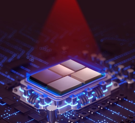
Illustration: Laser-Assisted Bonding (LAB)
LAB has been the preferred method for direct bonding of high-precision chips, offering several unique advantages in practical applications:
- High Precision: LAB leverages the high energy density and precise control capabilities of laser beams to focus on very small areas, overcoming the limitations of traditional bonding techniques when dealing with small sizes, complex structures, or special materials. This allows for micron-level or even nanometer-level bonding precision, meeting strict requirements for bonding location and strength. Compared to traditional techniques like mass reflow or thermal compression bonding (TCB), laser-based localized heating effectively prevents yield reduction caused by thermal expansion without requiring additional measures.
- Non-Contact: Unlike traditional mechanical bonding or thermos-compression bonding, LAB is a non-contact bonding method. The laser beam heats and melts the material surface, achieving bonding without mechanical damage or contamination, thereby improving the quality and reliability of the bond. This makes LAB particularly suitable for bonding fragile materials and miniature devices.
- High Speed: LAB enables rapid bonding with the laser energy being instantly transmitted to the bonding interface. Bonding time can be reduced to just a few milliseconds or even less, significantly improving production efficiency, making it ideal for mass production and high-output electronics manufacturing.
- Versatile: LAB can accommodate bonding requirements for various materials, including metals, semiconductors, ceramics, and glass, offering broad application prospects in the electronics packaging applications.
- Scalable: LAB can be combined with other packaging techniques, such as flip-chip and wafer-level packaging, to achieve more complex electronic packaging structures.
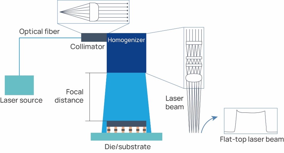
To ensure the quality and reliability, the LAB process requires precise control of key output specifications such as laser energy, uniformity, wavelength, and exposure time. Typically, an LAB system should include the following major parts to achieve the goal:
- High-Power Semiconductor Laser Source: Generates continuous output laser energy at a wavelength of 980nm.
- Optical Fiber: Transmits laser energy from the source to the optical shaping modules.
- Collimation Module: Collimates the laser beam to increase its directionality and focusing capability.
- Adjustable Homogenization Module: Produces a flat-top laser beam with adjustable width and length, ensuring uniform power density distribution across the beam. This ensures homogeneous heating of the bonding components, avoiding temperature inconsistencies caused by power distribution.
- Synchronous Temperature Control Unit: Monitors the temperature of the process area in real-time and controls the laser output in a closed-loop manner to ensure process consistency and stability.
On August 28, 2024, Focuslight officially launched the Flux H Series High-Precision Variable Laser System for Advanced Chip Packaging Processes, which offers the following features and advantages:
- Independently Adjustable Beam Size: Adaptable to requirements of different packaging structures with flexible processing solutions.
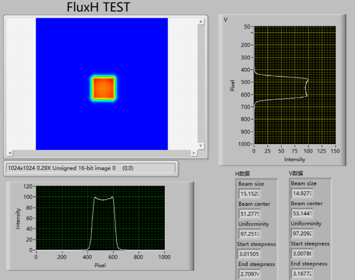
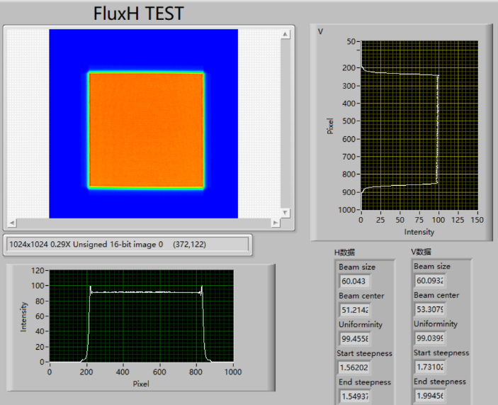
- High Beam Uniformity: A high uniformity standard of ≥ 95% across the entire beam area ensures bonding quality and process stability. No hot-spots in the beam that could reduce the process yield.
- Large Depth of Focus: Suitable for packaging processes involving multilayer and complex structures. This provides greater flexibility in handling different packaging heights and complexities.
- High-Accuracy Beam Center: Within the beam adjustment range, the system ensures high-precision beam positioning during the bonding, which is crucial for the packaging process requiring precise heat input control.
- Excellent Steepness at Beam Edge: A typical beam edge steepness of ≤ 3mm maintains a high energy concentration even at the edges of the processing area. It also effectively prevents overheating and reduces the thermal impact on sensitive surrounding areas.
-
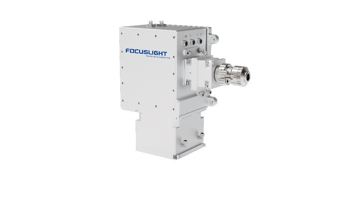
Flux H Series High-Precision Variable Laser System for Advanced Chip Packaging Processes
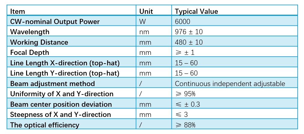
Key Specifications and Typical Test Results:
Focuslight’s newly launched Flux H Series High-Precision Variable Laser System offers highly efficient and reliable solutions for advanced chip packaging processes with its superior performance and versatile applications. The typical configuration of Flux H Series is now available for customer orders with customization possibilities aligning with customer needs. Through innovation, operations excellence, and fast response, Focuslight remains committed to be your globally trusted partner in the photonics industry.


 Return
 Download