Optical communication is one of the core technologies of modern society and plays a vital role in the world of Internet, data centers, mobile communications, and optoelectronic systems. With the rapid advancement of 5G, artificial intelligence, the Internet of Things (IoT), big data and cloud computing, optical communication technology has been rapidly evolving. Driven by exponential internet traffic growth and the future demands for data center interconnects, high power density and ultra-long-distance transmission, optical communication systems are now progressing along five major trends: higher bandwidth, lower latency, increased reliability, higher efficiency, and further miniaturization.

Optical modules, serving as an interface for optoelectronic conversion between devices and optical fibers, are essential for modern optical transmission networks. These modules are primarily composed of photon chips, optical components, circuit boards, and supporting materials (such as housings and pins). The optical components used in these modules have the major functions of collimation, coupling, or focusing, and they are usually made with materials including optical glass, fused silica, and silicon. Among these, silicon lenses have shown significant advantages over conventional glass lenses, making them a perfect fit for optical communication applications:
- Outstanding Optical Performance: Silicon lenses generally have a higher refractive index than glass. This allows silicon lenses to make more compact structures happen with similar optical designs, reducing the overall size and weight of the optical system. The high refractive index and optical transparency of silicon lenses can further enhance coupling efficiency using diffraction limited optical performance, reducing light transmission losses, and thus improve the overall energy conversion efficiency of the system. This is essential for optical communication, photodetection, and optical sensing applications.
- Cost Advantages: Silicon lenses, unlike glass lenses, can be manufactured using micro material processing techniques such as photolithography and etching, which are common in semiconductor manufacturing and offer cost advantages in mass production. Flexible and reusable masks used in the processing also help reduce initial With continuous advances in semiconductor manufacturing technology and materials science, the production cost of silicon lenses is expected to decrease further.
- Efficient and Flexible Manufacturing: Using wafer-level manufacturing technology, silicon lenses are made with high production efficiency, minimized material waste, and even lower production costs. This enables large-scale, high-consistency, and easily scalable mass production to meet the growing demand for optical components from the optical communication industry. Compared to the complex manufacturing processes of glass lenses, the production of silicon lenses is simpler and more efficient, shortening the design-to-mass-production cycle to quickly respond to market changes and meet customization needs.
For long-distance communication applications, where optical modules and components require higher precision, reliability, and stability, fused silica is a more suitable choice due to its unique advantages:
- High melting point (~ 1713 °C) and high thermal stability, enabling it to withstand high-temperature environments without deformation or damage.
- Fused silica has one of the lowest thermal expansion coefficients among refractory materials, helping prevent cracking or warping during temperature fluctuations, thus ensuring product stability and reliability.
- Low thermal conductivity is advantageous in applications requiring reduced heat transfer or temperature stability.
- Fused silica resists many chemicals, maintaining stable performance and reliability in harsh chemical environments.
Focuslight employs its core technology of photolithography and reactive ion etching in wafer-level precision optics manufacturing to mass-produce lenses and lens arrays with various optical materials and structures. This advanced technique, pioneered by Focuslight Switzerland, is a leading technology that produces precision micro-nano optical structures on wafers according to specific design goals, which is particularly suitable for mass production of micro-nano optical components in the field of optical communications.

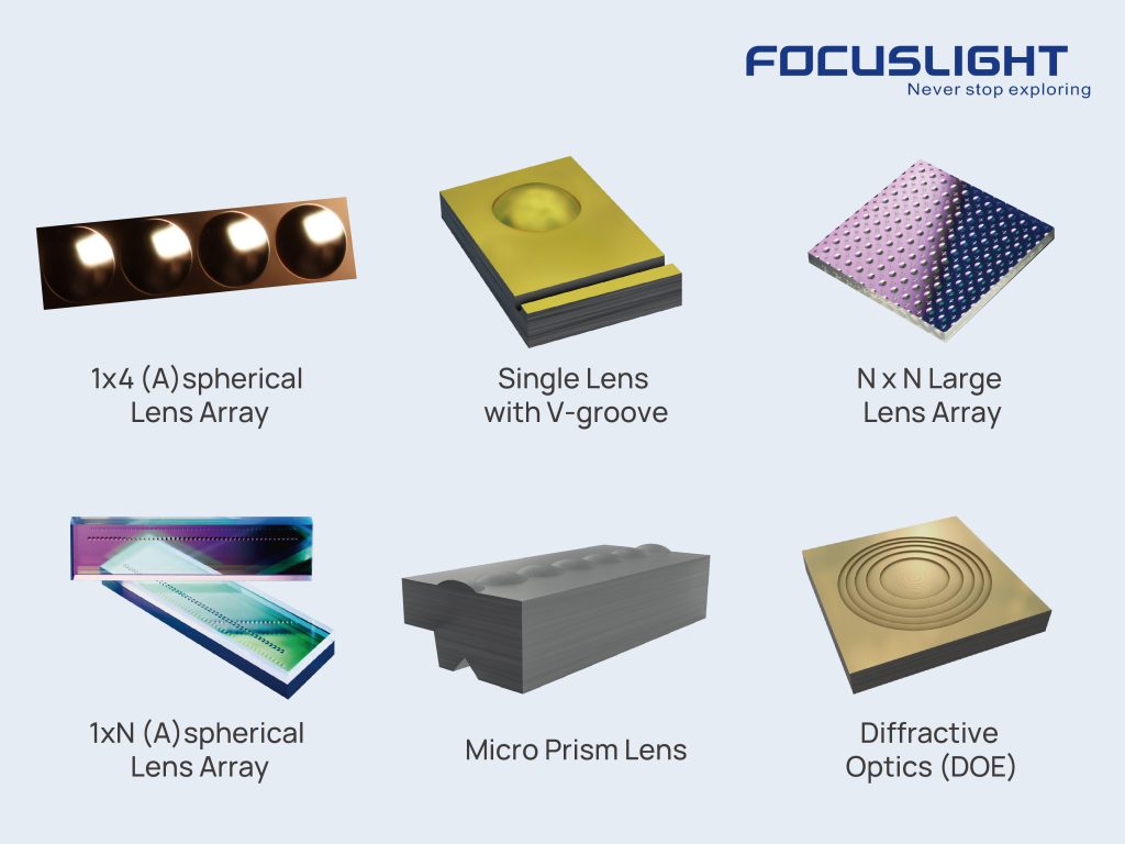
Focuslight utilizes industry-leading optical manufacturing technologies to provide customized services for the optical communications industry, offering a variety of lens types, shapes, and array configurations to meet diverse application needs.For example, Single Lens with V-groove, N×N Large Lens Array, 1×N (A)spherical Lens Array, Micro Prism Lens, and Diffractive Optics (DOE).On November 21, 2024, Focuslight Technologies released a series of standardized silicon and fused silica lenses, and lens arrays designed for optical communications.

Through close collaboration with our customers, we remain goal-focused and committed to advancing the development and implementation of innovative photonic technology solutions, fostering growth and shared success. Through innovation, operations excellence, and fast response, Focuslight strives to be your globally trusted photonics solution provider.


 Return


