As Photonic Integrated Circuits (PICs) continue to advance in data centers, AI computing, and other high-performance domains, achieving high-precision fibre-to-PIC coupling has become essential to improving system performance and enabling scalable manufacturing. This growing demand is driving the industry to seek next-generation interfacing technologies.
Recently, PIC Magazine, a leading international publication focused on optical communications and photonic integration, published a feature article by Focuslight titled “Reimagining PIC-fibre interfaces with engineered V-Groove technology.” The article examines how engineered V-groove arrays powered by wafer-level simultaneous structuring deliver breakthroughs in precision, throughput, reliability, and scalability, bringing new innovation and value to photonic integration and packaging.
Key Takeaways
The Hidden Bottleneck in PIC-Fibre Interfaces: Precision Meets Scalability
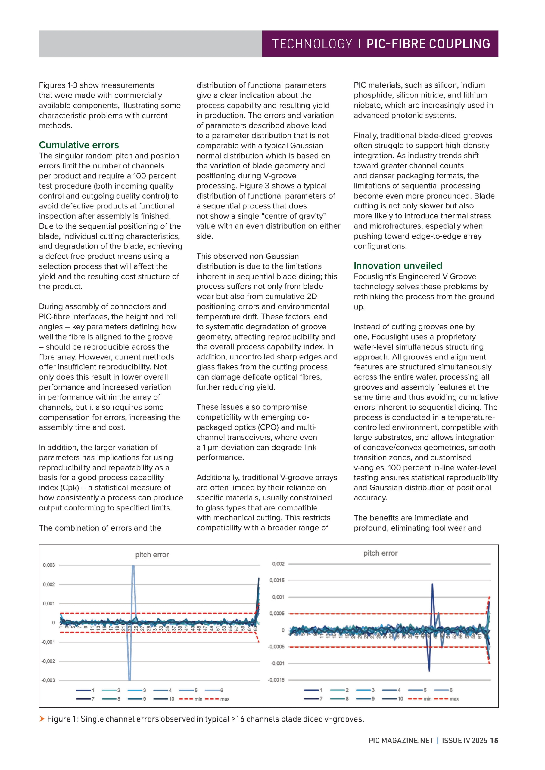
In data centers and AI computing, coupling accuracy and channel-to-channel consistency of PICs are becoming critical constraints affecting both performance and mass production. Traditional blade-diced V-groove processes — based on sequential cutting — struggle to simultaneously meet submicron alignment requirements and high-channel-count scalability. These limitations become even more pronounced in high-density architectures such as CPO.
Wafer-Level Simultaneous Structuring: A Structural Breakthrough
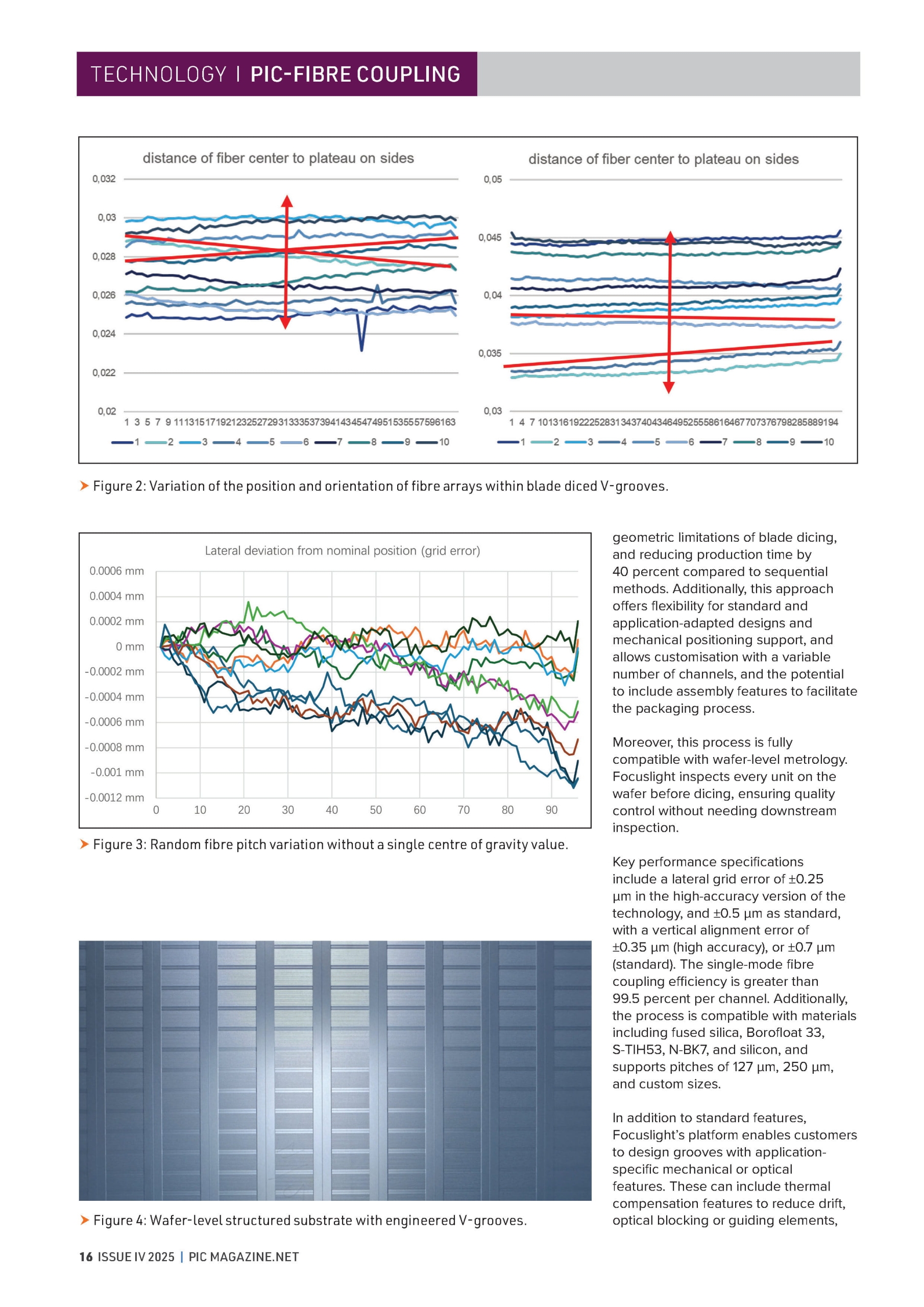
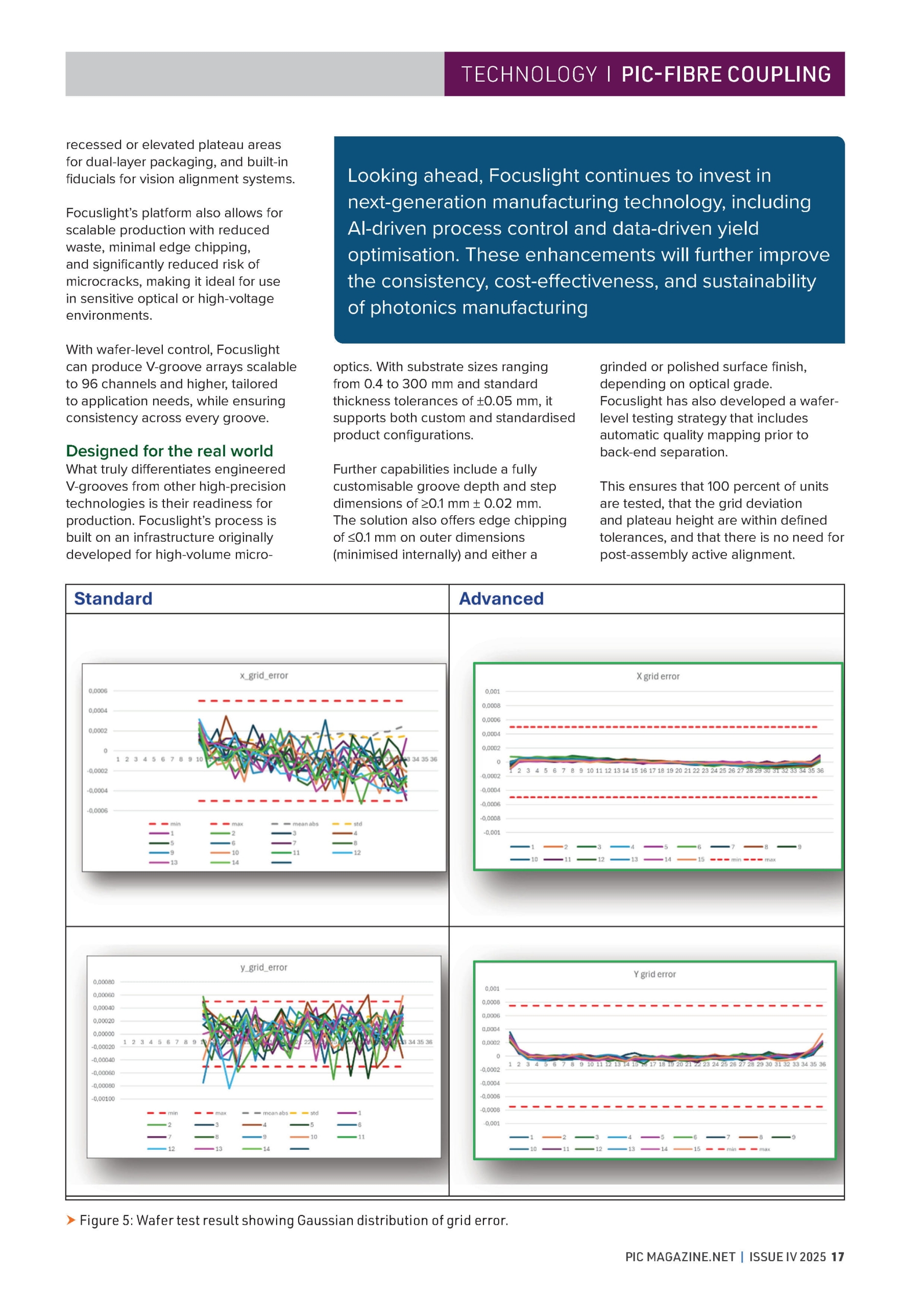
Built on a mature wafer-level manufacturing platform, Focuslight’s wafer-level simultaneous structuring approach forms all grooves and alignment features in a single process step across the entire wafer. This minimalizes cumulative errors inherent to sequential dicing, enables complex customized geometries, and supports high-density array designs. The result is a fundamentally improved solution for high-precision, high-volume photonic packaging.
Designed for CPO and the AI-Driven Future
The engineered V-groove platform maintains high yield, high uniformity, and compatibility with automated assembly, while supporting up to 96 channels and beyond across multiple substrate materials. These capabilities make it an ideal foundation for Co-Packaged Optics (CPO), AI computing, quantum communication, and other high-speed interconnect applications.
Guided by the motto “Engineered in Europe, Scaled in Asia – Accelerating Global Reach in High-Precision Micro-Optics,” Focuslight continues to advance wafer-level micro-optics technologies for large-scale deployment in optical communications, laying a solid manufacturing foundation for future high-density, high-performance photonic systems.
— Full article reposted below —


Please click here to visit the page of this article on PIC Magazine website, or refer to PIC Magazine Issue IV 2025, pp. 14–18.


 Return
